Active Components
Active components which have internal capacity to change energy format from one form to another hence reqire an external source whose operation can be controlled.
Semiconductors:
• Material whose conductivity lies in between conductor and insulator.Semiconductors are more like insulators in their pure form but have smaller atomic band gaps
• Adding dopants allows them to gain conductive properties
Doping
• Foreign elements are added to the semiconductor to make it electropositive or electronegative
• P-type semiconductor (postive type)
– Dopants include Boron, Aluminum, Gallium, Indium, and Thallium
– Ex: Silicon doped with Boron
– The boron atom will be involved in covalent bonds with three of the four neighboring Si atoms. The fourth bond will be missing and electron, giving the atom a “hole” that can accept an electron
• N-type semiconductor (negative type)
– Dopants include Nitrogen, Phosphorous, Arsenic, Antimony, and Bismuth
• Ex: Silicon doped with Phosphorous
– The Phosphorous atom will contribute and additional electron to the Silicon giving it an excess negative charge
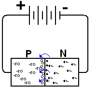
P-N Junction Diodes
• Forward Bias
– Current flows from P to N
Active components which have internal capacity to change energy format from one form to another hence reqire an external source whose operation can be controlled.
Semiconductors:
• Material whose conductivity lies in between conductor and insulator.Semiconductors are more like insulators in their pure form but have smaller atomic band gaps
• Adding dopants allows them to gain conductive properties
Doping
• Foreign elements are added to the semiconductor to make it electropositive or electronegative
• P-type semiconductor (postive type)
– Dopants include Boron, Aluminum, Gallium, Indium, and Thallium
– Ex: Silicon doped with Boron
– The boron atom will be involved in covalent bonds with three of the four neighboring Si atoms. The fourth bond will be missing and electron, giving the atom a “hole” that can accept an electron
• N-type semiconductor (negative type)
– Dopants include Nitrogen, Phosphorous, Arsenic, Antimony, and Bismuth
• Ex: Silicon doped with Phosphorous
– The Phosphorous atom will contribute and additional electron to the Silicon giving it an excess negative charge
P-N Junction Diodes
• Forward Bias
– Current flows from P to N
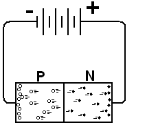
• Reverse Bias
– No Current flows
– Excessive heat can cause dopants in a semiconductor device to migrate in either direction over time, degrading diode
– Ex: Dead battery in car from rectifier short
– Ex: Recombination of holes and electrons cause rectifier open circuit and prevents car alternator form charging battery
Advantages:
• Less space consumption.
• Power consumed is less.
• Heat dissipated is less.
• Low cost
Transistor
• A transistor is a 3 terminal electronic device made of semiconductor material.
• Transistors have many uses, including amplification, switching, voltage regulation, and the modulation of signals.
• The word “transistor” is a combination of the terms “transconductance” and “variable resistor”.
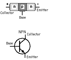
BJT Transistors
• BJT (Bipolar Junction Transistor)
– npn
• Base is energized to allow current flow
– pnp
• Base is connected to a lower potential to allow current flow
• 3 parameters of interest
– Current gain (β)
– Voltage drop from base to emitter when VBE=VFB
– Minimum voltage drop across the collector and emitter when transistor is saturated
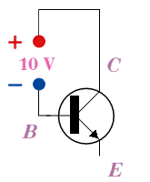
npn BJT Transistors
• High potential at collector
• Low potential at emitter
• Allows current flow when the base is given a high potential
• Less space consumption.
• Power consumed is less.
• Heat dissipated is less.
• Low cost
Transistor
• A transistor is a 3 terminal electronic device made of semiconductor material.
• Transistors have many uses, including amplification, switching, voltage regulation, and the modulation of signals.
• The word “transistor” is a combination of the terms “transconductance” and “variable resistor”.
BJT Transistors
• BJT (Bipolar Junction Transistor)
– npn
• Base is energized to allow current flow
– pnp
• Base is connected to a lower potential to allow current flow
• 3 parameters of interest
– Current gain (β)
– Voltage drop from base to emitter when VBE=VFB
– Minimum voltage drop across the collector and emitter when transistor is saturated
npn BJT Transistors
• High potential at collector
• Low potential at emitter
• Allows current flow when the base is given a high potential
pnp BJT Transistors
• High potential at emitter
• Low potential at collector
• Allows current flow when base is connected to a low potential
• High potential at emitter
• Low potential at collector
• Allows current flow when base is connected to a low potential
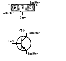
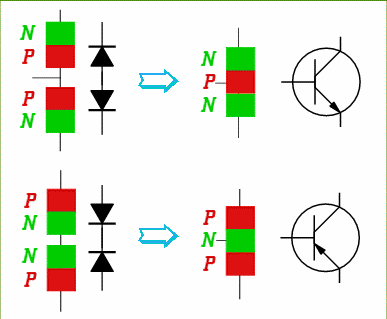
Bipolar Transistors
• Two PN junctions joined together
• Two types available – NPN and PNP
• The regions (from top to bottom) are called the collector (C), the base (B), and the emitter (E)
• Two PN junctions joined together
• Two types available – NPN and PNP
• The regions (from top to bottom) are called the collector (C), the base (B), and the emitter (E)
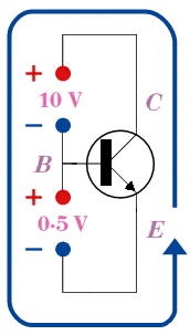
Operation
- Begin by reverse biasing the CB junction
- Here we are showing an NPN transistor as an example
- Now we apply a small forward bias on the emitter-base junction
- Electrons are pushed into the base, which then quickly flow to the collector
- The result is a large emitter-collector electron current (conventional current is C-E) which is maintained by a small E-B voltage
- Some of the electrons pushed into the base by the forward bias E-B voltage end up depleting holes in that junction
- This would eventually destroy the junction if we didn’t replenish the holes
- The electrons that might do this are drawn off as a base current
Transistor Amplifiers
Amplification
Ø The process of increasing the strength of a signal.
Ø The result of controlling a relatively large quantity of current (output) with a small quantity of current (input).
Amplifier
Ø Device use to increase the current, voltage, or power of the input signal without appreciably altering the essential quality.
